Mask for printed circuit boards at home. Homemade frame with stretched stencil mesh
The solder mask, or “green stuff” as it was previously called, protects the printed circuit board during soldering by covering the conductors, preventing short circuits between pads and protecting the fiberglass laminate from overheating during installation. Previously it was only possible to make it green. There are many colors available now. Which color should you choose? And does it make any difference what color of mask is chosen?
Examples from life
We have a customer who orders his own solder mask color for each type of printed circuit board. It all started with shades of blue, red, purple, then there was black, white, now purple, turquoise, burgundy...
There is another customer - a huge enterprise with many departments. Each department chooses its own mask color. In my opinion, even every developer at this enterprise prefers his own shade. Is it good or bad?
In my opinion, this is not just bad - it is a disaster for the enterprise. And that's why.
1. Problems with incoming control
If a facility performs incoming visual inspection of printed circuit boards, differences in mask color can lead to a significant increase in personnel fatigue. Firstly, bright colors, such as red or white, are significantly more tiring to the eyes. Secondly, as the color changes, the saturation of the mask also changes, which means it may be more difficult to distinguish the conductors underneath and control their quality. Thirdly, an eye accustomed to identifying defects under a mask of one color will not be able to find them with the same quality when changing colors.
2. Problems with installation and output control
Even greater difficulties begin during the final visual inspection after installation. Especially if the mask is black or white. Controlling the presence of components turns into a real pain. If small components such as 0402 are used, quality control of their installation against a dark or black mask can be lengthened several times.
3. PCB quality problems
The standard color of the mask is green. Accordingly, each printed circuit board production plant has a supply of masks of this color in stock. But as soon as the games begin with the choice of mask color and shade (“I’d like red, please, but not faded, but brighter...”), the manufacturer is forced to select the right mask either from its own stocks or from a materials supplier. And it may happen that the dilution, application or curing mode of this mask is slightly different from the standard one. And here a loss of quality of the mask coating is possible. So you need to change the color of the mask for large batches with caution, try samples first.
4. Problems with the appearance of printed circuit boards
I strongly advise against using a white mask. After installation in the oven, it acquires a “yellowish” tint.
I do not recommend using a red mask. The difference in shades is too noticeable, and when making repeats you may end up with a shade that does not in any way match the boards of the previous launch.
Black and blue boards look good, but, as I already said, they are much more difficult and take longer to control visually.
Matte and glossy
A glossy mask is more comfortable and scratches are less visible. Boards with a glossy mask look more elegant.
PCB technology makes a green glossy mask by default.
In some situations it is necessary to use special colors (for example, matte black is used in traffic lights to reduce glare, and white is used in illuminators to increase light output). In such situations, choosing a non-standard color or matte/glossy finish is quite justified.
The quality of any homemade electronic device very much depends on how well it is made
was manufactured (yes, it’s a useful phrase, it’s already clear! Well, yes... But I need to for some reason
begin?).
The printed circuit board plays a big role in this (unless you have a very simple design that
it is possible
make volumetric installation). The more complex the device, the more complex the printed circuit board design, and the more
better quality
it must be manufactured. About one of the ways DIY PCB making speech
and it will go.
Preface
All materials used in this article can be purchased in our store
There are several ways making a printed circuit board at home. At the very beginning (this was back when I was studying to become an electronics engineer at school), I painted paths with nail polish (the result was very brutal printed circuit boards), then I tried a waterproof marker (even better). But only when I mastered laser ironing technology(LUT) (and this happened relatively recently) I was finally able to get the quality of the boards that was pleasing to the eye. After all, I make electronic crafts purely for the sake of the process itself. Well, this is my hobby. What's the point in soldering something on a scary printed circuit board? But after a couple of years, this technology stopped suiting me. Although LUT has many advantages:
- speed (if I had a printer, I was able to achieve about 10 minutes from printing to starting soldering);
- simplicity (although you will have to pay for this simplicity with a good dozen unsuccessful takes at the very beginning of using this technology. That is, you need to “get better.”)
- good repeatability. (I succeeded in about 90% of all attempts. I did not include the first ten in the statistics!).
Using laser-iron technology, it was even possible to apply inscriptions, which is what I did in some cases.
But LUT gave an accuracy of no more than 0.3 mm. This is the practical ceiling. I tried to make the tracks thinner, and it worked, although at the same time the percentage of defects increased significantly. In general, I have already drawn out the preface to the article, so let’s move on to the solder mask itself.
What is a solder mask?
FSR8000- two-component composition sensitive to ultraviolet radiation. Has three states.
1. "Raw State". After the two components have been mixed. In this form, it can be washed off with either acetone or a solution of soda ash.
2) "Hardened State".
2a) Not exposed to ultraviolet light. Dissolves with acetone and soda ash solution.
2b) After exposure to ultraviolet light, the mask becomes resistant to soda ash solution, but can still be washed off with acetone.
3) "Baked state". It is obtained after heating to 160 degrees, followed by exposure for several tens of minutes. It is not soluble in acetone and has great mechanical resistance.
In simple terms: a mask is a protective layer that can often be seen on factory-made printed circuit boards. Very often green. This article will discuss the non-standard use of this mask as a photoresist.
To do this, you need to use the first two states, i.e. Using illumination and subsequent development, obtain a pattern of conductors on the PCB. And after etching, wash off this pattern with acetone.
Then the mask can be used for its intended purpose, covering the area of the entire board with a mask, except for the contact pads intended for sealing parts. Then transfer the mask to the third state. And now about the same thing, but in detail and with photographs.
List of what is needed for the PCB manufacturing process
- - FSR8000(You can buy in our store)
- Thermostat. Despite the menacing name, you can use a regular iron with the ability to adjust the temperature. You also need a thermometer (up to 160 degrees) to remember the positions of the regulator at 70 degrees and 160 degrees. After this, the thermometer will essentially no longer be needed.
- . You can simply use a regular energy-saving lamp with cold light. It’s just that the exposure time will be very long. But it's safe.
- Frame with mesh. Frame with stretched mesh.). for a mask and can be purchased on our website, we also recommend reading the article
- Photo template with the board design and placement of contact pads. for photo template,
- Insulin syringes. Needed to accurately mix the components of the mask .
- Toothpicks. For stirring the components of the mask.
- To uniformly apply the mask to the PCB we need: , credit card, piece of foam plastic. I use a credit card (no longer needed, of course).
- For development we need soda ash. Look next to washing powders in stores.
- Acetone. To wash off the mask after etching.
- Capacity for developing (any plastic container)
Technological process for making a printed circuit board at home
Photomask(). It can be done in a printing house that has equipment for phototypesetting films. Often this service is not advertised by printing houses, as it is purely internal. But, as a rule, they agree to print your handkerchief drawings onto phototypesetting film without any problems. The file format and dimensions of the drawings must be clarified with the specific printing house.
To obtain a board pattern, the template must be inverted (white tracks on a black background). For a protective mask – straight (black circles on a white background) .
Photoresist Ordyl Alpha 340
The photographs show the photomask itself. One side seems embossed, the other should be glossy and smooth.
It is important not to confuse the sides - the photo layer is on the side where the relief is. 

A wooden frame (made of balsa, glued with low-viscosity superglue!) with a stretched baby bow. 
We cut out the blank from PCB. We give some margin on the sides.

Clean the surface with sandpaper. You don't need to try hard, just remove the dirt. The mask has very good adhesion. 
The photo shows cleaned textolite. Metal shavings must be washed off with water.

Iron with a thermometer. It is not necessary to always control the process like this. Now I know the position of the regulator
for 60-80 degrees, and by setting it to this position, I am sure that I am getting the desired temperature.
Be careful, the iron temperature should not exceed 100! 
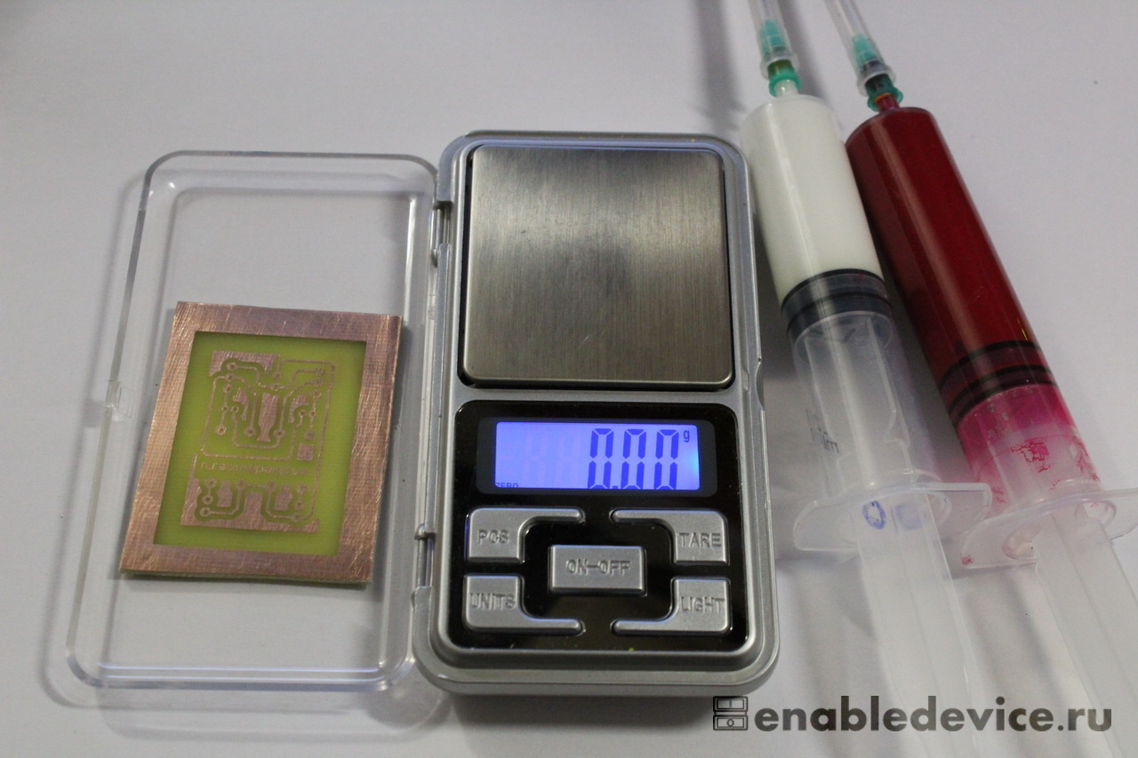
We collect the mask components into small syringes. 
Everything you need to get the job done
- mask components in syringes
- frame
- photo template
- toothpicks
- Squeegee rubber 
Squeeze the required amount of reagents onto the textolite.
For such a scarf, this is 3 ml of mask (green component) and 1 part of hardener (white component). Those. the proportion should be 3 to 1
.
Stir with a toothpick. We try to stir well, since a lot depends on the quality of stirring. 
Mixed homogeneous mask 
Press down with mesh on top. Here, perhaps, it is worth saying that in some cases (especially when
when the mask is already expired) it is better to mix large portions, for several at once
handkerchief. Then place a frame with a mesh on the scarf, and apply the required amount of mixed mixture on top of the mesh.
masks. Then the mesh will not allow dense (thickened) lumps of the mask to get onto the PCB, thereby spoiling
the whole picture. 
We distribute the mask over the textolite. The point is that the mask remains only in the grid cells. Then when removing
mesh - we will get a uniformly distributed mask. Therefore, use a piece of squeegee rubber (or a credit card)
We try to remove excess mask from the surface of the mesh. Without fanaticism! Don't tear the mesh 
Result 
Carefully remove the mesh 
The mask quickly spreads over the entire surface, forming a uniform layer 
Place the scarf on the iron 
Cover the scarf with something to protect it from dust. And wait a few minutes (or tens of minutes).

Meanwhile, we throw the mesh with traces of the mask into soda ash. 
It is important to catch the moment when the mask is almost completely dry. You can try checking the mask with your finger on the edge of the scarf.
(where you left the clearance. You left the clearance, right?!). If, when you pass your finger on the surface, there is no
traces, and the mask slightly sticks to the fingers - this is what we need. Scarf with a mask with a cut out pattern. 
We apply the template with a photo layer to the mask and carefully smooth it to the scarf. DO NOT CONFUSE THE SIDE! If the surface
a little sticky - the template sticks to the scarf without any problems. If the surface is already almost dry, it doesn’t matter.
Try either moistening the surface with water so that the template sticks, or using something to press the template onto the scarf.
(You can wrap it with tape. But be careful!) In general, the template should fit snugly to the scarf.

We put it in the light. The exposure time is determined experimentally. I can tell you my lighting modes:
70 (or even 80) minutes at a distance of 7 cm, under a 22-watt energy saver. A UV lamp will give much less
exposure time, but at the same time the time tolerances will correspondingly decrease). 
Preparing the solution for development 
Water at room temperature. Cleaned, soft. Dosage – experimental, in the photo the dosage for
soft St. Petersburg water (As you may have guessed, the photographs were taken by Termite). For hard water - soda should be
more. The solution should be slightly soapy to the touch. If there is too much soda, development will be fast,
but at the same time, the slightly underexposed mask will “peel off” during development. And if there is too little soda, the development will be
very slow. Moreover, heating the solution will only interfere with development. After the time required has passed
for exposure - remove the film and throw the scarf into the solution 
Scarf in solution. 
If everything is correct, then within a minute you should see a light pattern of conductors.

When the scarf has completely developed, wash it to remove any remaining soda ash and place it on the iron to dry. 
What happened. 
One of the unpleasant features of the mask is the underdeveloped areas.
On a dry scarf, they are very clearly visible as whitish spots. They shouldn't exist! They won't give the solution for
etching to get to the copper. Then we throw the scarf back into the solution and lightly clean those areas with a cotton swab.
Again, wash off, dry, control. And if everything is in order, then... We poison the scarf. 
During the etching process, we check that there are no air bubbles. Often they are located between the tracks. 
We poison, we poison... 
This is what happened 
Wash off the mask with acetone. You can check the scarf, ring for breaks and short circuits. After all, we will now
apply a protective mask, and then it will be very difficult to correct breaks, and especially short circuits.
Apply the mask template. The accuracy of the registration can be checked against light (if the scarf is one-sided) 
Again into the light (yes, yes, again for 70-80 minutes, if you don’t have UV. But you can make several scarves at the same time!)
Then go into development in the same soda ash solution. In principle, it lasts for a long time. It's true to change everything
it will have to be the same, because in the green solution you cannot see the scarf itself, and how it is made more and more beautiful 
For example, I like to watch how shiny copper pads gradually appear on a green surface 
So, pros using this method on your own PCB manufacturing:
- Very, very technologically advanced and beautiful
- High accuracy. 0.15 mm is not a problem. Two tracks between the legs of the DIP package? If you try, it's not a problem.
- Almost 100% repeatability(of course, this is when you already know at what distance and for how long to illuminate other small things, determined experimentally in the first attempts to make a scarf)
- Protective mask. This is a very good plus - after all, soldering with a protective mask becomes very simple - SMD components simply fall into place themselves.
And now the cons.
- A very long time. When using conventional energy saving devices - it takes a VERY LONG time. But who is stopping you from making scarves in batches?
- You need photosetting film. (You can, of course, use templates from a printer. But..., honestly, I don’t recommend it. Because then the tolerances for exposure time become very, very small)
Safety precautions.
Keep in mind - in the description of the FSR8000 a lot of unpleasant things are written about the toxic properties of the mask vapors. At a minimum, work with the window open. And best of all - under the hood. Now regarding my advice “touch it with your finger to see if it’s dry” - it’s still better not to do this. If you get the mask on your hands, wash it off quickly.
Acetone. Also harmful. It dissolves fat, which means it can do something unpleasant with subcutaneous fat. It is better to avoid prolonged contact.
Ferric chloride. It is better not to inhale its fumes. In general, my whole process takes place on the balcony, with the window open. I go onto the balcony only when my presence is necessary. And after finishing, I ventilate it well.
conclusions
Make DIY printed circuit board almost factory quality at home- perhaps, and not even very difficult! I would also like to master the high-quality production of vias...
With any factory board, the main difference will immediately catch your eye: on almost all factory boards, the tracks are covered with some kind of protective layer, only the contact pads remain on the outside. This layer can be green, red, blue, and sometimes even black or white. So what is it and why is it needed?
This coating is called a solder mask, and is designed to protect the tracks from oxides, accidental short circuits and overheating of the PCB during installation of elements. In addition to this, installing elements on a board covered with a solder mask is much more comfortable: the solder does not stretch along the tracks. If the parts are sealed with a hairdryer, then this is even more important. And the board with a mask looks much more attractive.
At the moment, three types of solder mask are available to the radio amateur:
- One-component (UV curing).
- Two-component.
- Dry film.
The one-component mask offered by our little Chinese friends is actually a repair paint. For example, it is very convenient for her to cover up the area where the paths are being restored. No, it is also used as a mask; in this case, an oven is not needed (and UV lamps are needed in any case), but in terms of strength it is still inferior to a two-component one. There is also a true one-component solder mask, but it is much less common.
The film mask is very similar to photoresist both in appearance and in the principle of working with it. Yes, yes, a protective coating can also be made from photoresist, but in reality it is only a semblance that has neither chemical nor mechanical strength. It is also quite rare, quite expensive, and most importantly, for full operation you need a vacuum laminator (for the mask to fully adhere to the surface of the board).
The most optimal price/quality ratio is a two-component solder mask. It is possible to purchase it by weight, which makes the mask even more affordable.
| Stores and sellers whose services I use. | |
|---|---|
| Online store "Everything for printed circuit boards" | Here we have repeatedly purchased a solder mask, a stencil mesh (and glue for it), squeegee rubber, and carbide drills. Photoresist is also purchased here. There are no complaints about the store, everything is packaged perfectly. There was only one peculiarity - orders took quite a long time to be collected and sent (most likely, one person did this). Now (09/13/2017) the store is changing its owner, what will happen next - time will tell. |
| Maxim (nickname: smacorp) from the RadioKot website. | An excellent seller and just a pleasant person to talk to. Here you can purchase liquid tin for chemical tinning and a soldering mask. All this is of excellent quality. |
Yes, applying a solder mask makes the board manufacturing process even more labor-intensive, time-consuming and requires new tools and materials. But a real radio amateur should not stand still; acquiring new skills and knowledge is always good.
As usual, let's divide the board manufacturing process into stages:
Drilling the workpiece, applying photoresist, exposure, development, etching. We covered all these stages earlier. Perhaps someone will be surprised by the fact that the first stage is drilling, usually we did this almost at the very end, but in this case the holes are drilled by a CNC machine, and the order will be exactly like this. We will talk about preparing files for the machine and making a board using it, but for now we will take this as a given.
Drilled blank with photoresist applied.

Preparation before exposing the tracks.
In the second photo you can see that next to the track template there is another template (in fact, there is more than one). This is the template for the solder mask. According to the principle of working with it, the mask is not much different from photoresist. This is exactly the same photosensitive material, with minor differences: it consists of two components and it is liquid.
Mixing the mask. Before applying the mask, the composite and hardener are mixed in a certain proportion, for example, for the FSR-8000 mask - 3:1. The composite has the color of the coating, and the hardener is white.
 All you need.
 The situation when there is not enough mask during application has a very depressing effect on the psyche, which means it is necessary to calculate its quantity. In fact, everything is simple here: for 1 square decimeter of the board (10*10 cm), 2 grams of mask is enough with a margin. Of course, it all depends on the consistency and method of application, but I’m talking about a situation where the mask is not diluted with anything (thick enough) and is applied through a special mesh using a squeegee. Yes, quite a small expense.
For example, our workpiece measures 6.5 cm by 4.5 cm. We calculate the area in decimeters: (6.5 cm * 4.5 cm) / 100 = 0.2925 dm². We believe that 0.3 dm², in our case it is better to round up. We count the amount of mask: 0.3 dm² * 2 g. = 0.6 g. This is the quantity of the finished mask. Since we mix in a ratio of 3 to 1, then 0.6 g. / 4 parts = 0.15 grams - the weight of one part. This means that 3 parts of the composite weigh 0.45 grams, and one part of the hardener weighs 0.15 grams. We interfere.


There is nothing wrong with the fact that there is a hundredths of a gram more of the composite than it should be. But if we are talking about a situation where there is more of something, then it is very desirable that it be a composite and not a hardener. Again, by hundredths, no more, proportions must be observed. Next, mix the mask very thoroughly and leave for a few minutes. In the meantime, let's prepare the grid.
Applying a solder mask. There are two requirements for applying the mask: the layer must be thin and necessarily uniform. You can, of course, try to cope with improvised means (here usually paint rollers, spatulas for sealing joints and other garden tools are used), but still the only correct way is to apply it through a stencil.
Stencil mesh is a material perfect for applying a mask. I use LM-PRINT brand meshes (the link to the store is in the table above). The mesh markings indicate the number of threads per cm and the diameter of the threads in microns. For example, LM-PRINT PES 61/60 PW - 61 threads per cm, thread diameter 60 microns. The lower the number of threads, the thicker the mask on the surface of the board. And vice versa.
For the mesh, you can find special frames on sale on which the mesh is stretched. In my case, this is a regular 18 mm profile pipe. There is a special glue for the mesh, purchased in the same place where the mesh is purchased. You can read about tensioning the mesh. The posts at the corners of the mesh raise it above the workpiece by 3 mm.

The perimeter of the workpiece is glued onto the mesh with masking tape. Let's prepare two windows at once: for the mask and for silk-screen printing. The squeegee rubber is also special, and was purchased in the same place as the mesh.

The prepared mask is applied in an even layer to one side of the board. After which, in one confident movement, it is pulled along the workpiece with the edge of a squeegee located at an angle. The main thing is not to stop when applying. Of course, experience is needed here, and over time the result will only get better. And for training you can use toothpaste, for example.


Drying the solder mask. A very important stage. When making a solder mask, the board blank has time to go through the oven twice. The first time is for pre-drying and the second time is for final curing. And there is only one difference - temperature. If drying is performed at a temperature of 75-85°C, then tanning is at 150-160°C. Can you guess what will happen if you exceed the pre-drying temperature? Yes, the mask will completely harden, and it will be impossible to wash it off with any developing solutions. We will receive a board with a beautiful and even mask, which is completely unsuitable for soldering, since the mask layer is solid. All that remains is to throw it away, and this is the entire cycle from applying the photoresist to the essentially finished board. It's a shame? Of course. That’s why we pay very close attention to drying. Of course, it is better to entrust such a task to units designed for this purpose. I have a furnace for this, with a PID controller installed in it. Pre-drying usually takes 30-55 minutes. The main thing is that the mask should not stick after drying. Moreover, while it is hot, such an effect can exist, but when it cools, it should disappear.

Solder mask exposure. It differs from photoresist only in the exposure time, otherwise everything is exactly the same. The mask is negative (like photoresist, what was exposed is polymerized), which means we cover only the contact pads. Next we exhibit.


Solder mask development. Again, everything is the same as with photoresist. Even the solution is the same, so after developing the photoresist we don’t pour it out, but use it further. And even after developing the mask, it will be useful; we will use it to develop the silk-screen printing and wash the mesh from the mask. I would like to draw your attention to this: if the mask is glossy, then during development this gloss can easily be damaged, so ideally you should not touch the surface of the board at all. However, if everything is done correctly, the mask appears very easily.

Silk-screen printing. In principle, marking the elements on the board is not the most necessary thing. If in some cases it’s completely depressing without a solder mask, then the designation of elements is simply a convenience when assembling the device. So let's apply the markings. For this we use the same mask, just select the blue color.
note
If the marking is applied on the same side as the solder mask, it must be tanned for at least 15 minutes at the appropriate temperature. If you apply a new layer to a mask that is not tanned, the solvent included in the mask will damage the bottom layer. The mask remains on the board, but its surface cracks. Moreover, if the color of the silk-screen mask is white, these cracks are ultimately very visible.
We have markings on the reverse side, so application without drying is acceptable. Mix the blue mask in the same way and apply it to the back side of the board.

Drying silk screen printing. Place in the oven for 45 minutes at a temperature of 75-85°C.
Silkscreen display. We only need to designate the elements, which means we use a negative template.

Silk screen printing development.

Final drying. Performed at a temperature of 150-160°C for 45-75 minutes. At this temperature the mask gains its final strength.
While the board is drying, you can wash the mesh from the mask. A developing solution of soda ash and a dish sponge can easily cope with this.

Trimming the board. Of course, it is not at all necessary to do this using a machine, but since he drilled the holes, then let him also cut along the contour.

Tinning. There is also one feature here: after the furnace, the copper on the contact pads is oxidized, and it is not so easy to tin. But this can be fixed very easily; just dip the board in water with citric acid added for a minute. We use it for etching, so this is not a problem. Half a teaspoon in half a glass of water is enough, and the copper will become clean and shiny.
The series of articles on device manufacturing has come to an end. As I promised, we have come quite a long way. Of course, manufacturing is not limited to the considered methods; this topic is very extensive. But I hope the cycle allows you to get a general idea.
There are dozens of years between the first and last technologies. But that's not even the main thing. Between them is the enormous work of the whole world of radio amateurs. Work full of experiments, victories and mistakes, because only those who do nothing make no mistakes. Don't be afraid to ask questions, experiment and share your experiences (even if they aren't always successful). This experience will definitely be useful to someone else, it cannot be otherwise.
All the best.

This article is devoted to the manufacture of a homemade printed circuit board with green paint.
General issues of making printed circuit boards at home are fairly well covered on the Internet. I will not describe what others have already written a hundred times. Instead, I'll briefly describe my little tricks and processes, especially about vias and masking.
Homemade board 8 mil tracks, 6 mil distance, adapters and mask.
Equipment
Laser printer (Kyocera FS-1100 printer, for toner transfer), laminator, microcompressor.
Materials
Everything is as usual (textolite, ferric chloride, acetone, etc.) except for stained glass paint (Pebeo Vitrea 160).
Process
Sverlovka: Since I use CNC for drilling, the process occurs before the toner transfer, in this case it is easier to position the pattern. 

Transferring toner to the board:
Many people use an iron, but still, the best results were achieved using a laminator. We roll it through the laminator 10-15 times. Paper - everyone can experiment here too, I use 130 g/m photo paper. Using photo paper, it seems to me, increases the life of the printer itself. Printing mode, select the maximum toner consumption) Unfortunately, the trend is that modern printers are more and more economical (or fortunately, depending on which side you look at) and the thickness of the toner after transfer tends to decrease. This is what happened after the laminator:
![]()
Etching:
The etching process takes place in a ferric chloride solution and is no different from classical methods - warmer water, more iron, stir more often)
Vias:
Vias are an integral part of the process of making a homemade double-sided board. You can consider several options for homemade transitions:
1. Use of special bushings. Difficult to find or make. The need for a sufficiently large diameter in VIA.
2. Installation of jumpers using wire. It has one drawback - when the adapter is located under the housing of the SMD chip. This requires some experience. (experience is necessary everywhere, but making jumpers of the required length and then soldering them with a minimum amount of solder is sometimes not easy)
3. Pressing. This method allows you to create a high-quality transition connection between layers. For this purpose, a special press machine was created. Details about the press can be read in.

 It would seem that the next step is to earn the payment and go ahead! But no, it's boring and ugly. We are not looking for simple ways. Making a board with greenery
Mask
The mask protects the board from corrosion, creates more favorable conditions during installation, and gives the board a “branded” look. This is the first time anyone has read about a homemade mask. It is based on publicly available stained glass paint. Pebeo Vitrea 160. Water-based paint has one peculiarity - it requires firing (drying) in an oven at a temperature of 160 C for 40 minutes. In fact, I have not tried to fry the board above 130 degrees. A temperature of 130 is quite enough for normal paint polymerization.
First, we print a layer on the same laser printer to protect the pads involved in the installation. Simply put, we cover the necessary areas from the mask. Place it on the board and put it back into the laminator:
![]() Then we apply paint using our mini sprayer. I add 1 part water to 4 parts paint before applying. After application, wait 24 hours for the paint to dry. There is no need to rush - we will always have time to burn the board). After that, we kick my wife out of the kitchen and occupy the stove for 40 minutes. In fact, it is better to get some kind of mini-oven or use a toaster for these purposes. But in any case, you need to carefully monitor the temperature. After 40 minutes, remove the pie from the oven:
Then we apply paint using our mini sprayer. I add 1 part water to 4 parts paint before applying. After application, wait 24 hours for the paint to dry. There is no need to rush - we will always have time to burn the board). After that, we kick my wife out of the kitchen and occupy the stove for 40 minutes. In fact, it is better to get some kind of mini-oven or use a toaster for these purposes. But in any case, you need to carefully monitor the temperature. After 40 minutes, remove the pie from the oven:
 The protective layer, consisting of toner, is removed using a solvent or acetone using a slight mechanical force of the hands. The paint falls off from the protected areas due to poor adhesion to the toner. Now you can tin the pads and solder some SDR transceiver or other trinket. In general, the whole method is quite labor-intensive and is necessary, I believe, for very important trinkets. Well, or for real aesthetes who are not used to paying 1000 rubles for a branded double-sided board in China (if anyone is interested, write, I’ll give you the address of the site where you can actually order normal boards for 1000 rubles)
15.10.2015
Solder mask (Solder Resist or Solder Mask) is a mandatory heat-resistant protective coating for the conductive pattern of printed circuit boards. Purpose: protection of individual areas of the PP from the adverse effects of flux and solder, as well as the influence of a humid environment and mechanical stress.
Type variety
Application Features
The solder mask is applied to either one () or both sides of the PCB. It is necessary to insulate the contact areas (for the output of the microcircuit, etc.) from conductive elements - conductors or transition-type holes. The result is a reduction in labor intensity/soldering time.
If it is necessary to isolate adjacent contact areas, the cutout method is used (creating an area not covered with a solder mask layer). In this case, the size of the cutouts should be 100-150 microns larger than the total size of the contact area. The distance from one edge of the solder mask to the other edge of the contact area should be within 50-75 microns. The minimum width of the jumper - the area between 2 adjacent contact areas - is 75 microns.
The color - red, white, green, blue, black, yellow or super white - is chosen by the customer. In the LED industry, super white/white solder mask color is used, in other fields green is the most popular color. It should be taken into account that the final color saturation of PP is created not by the base material, but by the mask coating.
The process of creating a protective layer
The mask is applied through a stencil in the form of a mesh (the size of one cell is 150 microns). Wet layer thickness: 30-35 microns. Then, the product is dried. Temperature in the drying chamber: no more than 75˚. The dried blanks are sent to the stage of photolithography - combining photo masks of masks with products - and high-power UV exposure. The final stage is the development of the blanks in solution (substance temperature 32-34˚).
Restrictions
- When creating a thin bridge (less than 75 microns), it can be damaged during installation and disrupt the required adhesion to the surface of the PCB. The result is a loss of solderability properties of damaged contact areas.
- Inability to apply a mask to connector end contacts/test points.
- When creating a protective layer on printed circuit boards with a lead pitch of more than 1.25 mm, the solder mask is allowed to hit the contact areas only on one side and no more than 50 microns. And with a pitch of less than 1.25 mm - no more than 25 microns.
- All vias that are subject to subsequent solder mask coating must be covered (tented).
- Possible defects: presence of areas with no protective mask - less than 0.2 mm 2 on 1 conductor and less than 2 mm 2 on polygon areas; the presence of minor detachments (up to 0.25 mm); the appearance of long tunnel voids.
Pros of using a solder mask
- High chemical resistance . The mask protects against aggressive environments and oxidation of copper conductors.
- Significant indicators physical stability . There is protection against scratches and mechanical impact.