All modifications of the amateur transceiver have a quartz filter. Transceiver with crystal filter
The electrical circuit diagram of the main transceiver board is shown in Fig. 1.
In receive mode, the signal from the bandpass filter is supplied to pin 3 of the board, and then, through matching transformer T1, to the input of the first mixer DA1. The signal from the smooth range generator (VFO) is supplied to pin 6 of the microcircuit through the contacts of relay K1. The load of the mixer is an electromechanical filter (EMF) of the upper or lower sideband of the intermediate frequency Z1. The EMF is connected through a balun transformer T2. The cascade on the field-effect transistor VT4 provides amplification of the intermediate frequency (IF) signal. From the output of the amplifier, the signal goes to the second mixer (DA2). Through the contacts of relay K2, a signal from a reference frequency generator of 500 kHz is supplied to pin 6 of the microcircuit. The low-frequency audio signal is fed through a simple low-pass filter using C23R25C28 elements to the DA4 audio amplifier, assembled on an LM386. The amplifier is covered by an AGC circuit. The detected audio signal controls the resistance of the drain-source transition of transistor VT6, thereby providing adjustment of the audio signal level at the input of the DA4 chip. The output of the microcircuit is loaded onto a resistor - a volume control with a resistance of 100-680 Ohms. Low-impedance headphones are connected to the resistor motor.
To switch to transmission mode, a voltage of 12 V is applied to pins 6 and 9 of the board. In this case, relays K1 and K2 are activated and the microphone amplifier on transistor VT2 is turned on. The electret microphone is connected to pin 1 of the main board. The audio signal from the output of the microphone amplifier goes to the first mixer DA1. Resistor R4 serves for precise balancing of the mixer in transmit mode. On pin 6 The mixer receives a 500 kHz signal from the reference oscillator through the contacts of relay K1. The generated IF signal with a suppressed carrier is sent to the EMF, where the non-working sideband and, additionally, the remainder of the carrier are suppressed. On the pin. 6 DA2 receives a VPA signal. From the output of the microcircuit, the amateur band signal goes to pin 10 of the main board and then to the bandpass filters of the transmitter. The input of the audio amplifier DA4 in transmit mode is short-circuited by the open junction of transistor VT5. The reference frequency generator is assembled on transistor VT1 according to a capacitive three-point circuit. The 500 kHz signal is removed from capacitor C10 to the emitter follower on transistor VT3. The mixer chips and the reference oscillator are powered by a separate DA3 stabilizer.
Details and design.
The main board is assembled on a PCB board with double-sided metallization. The dimensions of the board are 52.5x120 mm (Fig. 2).
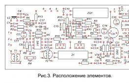
The top layer of metallization serves as a screen and is connected to the “negative” terminal of the power source. Metallization around holes not connected to the negative is removed. The arrangement of elements on the printed circuit board is shown in Fig. 3.
The design of the main board uses constant resistors such as S1-4, S2-23, MLT; tuning – SP4-1A. All permanent capacitors – K10-17, KM; electrolytic – K50-35. Transformers T1...T3 are made on K7x4x2 rings with a permeability of 600NN. The number of turns is indicated in the diagram. Winding is carried out with a wire with a diameter of 0.25 mm. The coils are placed in the screen. Relays K1 and K2 - RES49 with a winding resistance of 270 Ohms. Choke L2 is small-sized, with an inductance of 100 μH. Such chokes were used in domestically produced VCRs. Electromechanical filter - FEM4-52-500-2.75 or FEM4-52-500-3.1 with upper or lower side strip, manufacturer - Avers company.
Path setup.
The main board connection diagram is shown in Fig. 4.
A correctly assembled board in receive mode does not require configuration. In transmit mode, use R4 to set the maximum carrier suppression.
If necessary, using R13, the transmission coefficient of the microphone amplifier is selected so that even when loud sounds are uttered in front of the microphone, signal clipping does not occur. The signal shape can be monitored using an oscilloscope at the output of the power amplifier. If a dynamic microphone is used, elements R1, R2, R5 and C2 do not need to be installed. The optimal amplitude of the GPA voltage at pin 4 of the main board is 150…200 mV.
In transmit mode on pin 10 of the main board, the level of the useful SSB signal is 20-50 mV into a 50 Ohm load.
You can take a printed circuit board in Sprint Layout 5 format.
The appearance of the assembled main board is shown in the photo.
Literature
1. Double balanced mixer SA612A. Radio, No. 4, 2004, pp. 48-49.
2. Transceiver "Amator-EMF". Radioamator, No. 11, 1996, pp. 18-19
3. Transceiver “Amator-EMF-U”. Radiohobby, No. 5, 2000, pp. 33-38.
4. Main board of the "Amator-EMF" transceiver. Radiohobby, No. 6, 2007, pp. 37-38.
UR5VUL Alexey Temerev Svetlovodsk, Ukraine. 2008
At one time, the author proposed several options for simple transceivers using K174PS1 mixer microcircuits. The proposed main transceiver board uses imported SA612 microcircuits. EMF is used as a main selection filter. The main board is designed for a transceiver for amateur radio bands 160...40 M.
The circuit diagram of the main transceiver board is shown in Fig.1.
In receive mode, the signal from the bandpass filter is supplied to pin 3 of the board, and then, through matching transformer T1, to the input of the first mixer DA1. The signal from the smooth range generator (VFO) is supplied to pin 6 of the microcircuit through the contacts of relay K1. The load of the mixer is an electromechanical filter (EMF) of the upper or lower sideband of the intermediate frequency Z1. The EMF is connected through a balun transformer T2. The cascade on the field-effect transistor VT4 provides amplification of the intermediate frequency (IF) signal. From the output of the amplifier, the signal goes to the second mixer (DA2). Through the contacts of relay K2, a signal from a reference frequency generator of 500 kHz is supplied to pin 6 of the microcircuit. The low-frequency audio signal, through a simple low-pass filter using C23R25C28 elements, is fed to the DA4 audio amplifier, assembled on LM386. The amplifier is covered by an AGC circuit. The detected audio signal controls the resistance of the drain-source transition of transistor VT6, thereby providing adjustment of the audio signal level at the input of the DA4 chip. The output of the microcircuit is loaded onto a resistor - a volume control with a resistance of 100-680 Ohms. Low-impedance headphones are connected to the resistor motor.
To switch to transmission mode, a voltage of 12 V is applied to pins 6 and 9 of the board. In this case, relays K1 and K2 are activated and the microphone amplifier on transistor VT2 is turned on. The electret microphone is connected to pin 1 of the main board. The audio signal from the output of the microphone amplifier goes to the first mixer DA1. Resistor R4 serves for precise balancing of the mixer in transmit mode. On pin 6 The mixer receives a 500 kHz signal from the reference oscillator through the contacts of relay K1. The generated IF signal with a suppressed carrier is sent to the EMF, where the non-working sideband and, additionally, the remainder of the carrier are suppressed. On the pin. 6 DA2 receives a VPA signal. From the output of the microcircuit, the amateur band signal goes to pin 10 of the main board and then to the bandpass filters of the transmitter. The input of the audio amplifier DA4 in transmit mode is short-circuited by the open junction of transistor VT5. The reference frequency generator is assembled on transistor VT1 according to a capacitive three-point circuit. The 500 kHz signal is removed from capacitor C10 to the emitter follower on transistor VT3. The mixer chips and the reference oscillator are powered by a separate DA3 stabilizer.
Details and design.
The main board is assembled on a PCB board with double-sided metallization. Board dimensions 52.5x120 mm ( Fig.2).
The top layer of metallization serves as a screen and is connected to the “negative” terminal of the power source. Metallization around holes not connected to the negative is removed. The arrangement of elements on the printed circuit board is shown in Fig.3.

The design of the main board uses constant resistors such as S1-4, S2-23, MLT; tuning – SP4-1A. All permanent capacitors – K10-17, KM; electrolytic – K50-35. Transformers T1...T3 are made on K7x4x2 rings with a permeability of 600NN. The number of turns is indicated in the diagram. Winding is carried out with a wire with a diameter of 0.25 mm. The coils are placed in the screen. Relays K1 and K2 - RES49 with a winding resistance of 270 Ohms. Choke L2 is small-sized, with an inductance of 100 μH. Such chokes were used in domestically produced VCRs. Electromechanical filter - FEM4-52-500-2.75 or FEM4-52-500-3.1 with upper or lower side strip, manufacturer - Avers company.
Path setup.
The main board connection diagram is shown in Fig.4.

A correctly assembled board in receive mode does not require configuration. In transmit mode, use R4 to set the maximum carrier suppression.
If necessary, using R13, the transmission coefficient of the microphone amplifier is selected so that even when loud sounds are uttered in front of the microphone, signal clipping does not occur. The signal shape can be monitored using an oscilloscope at the output of the power amplifier. If a dynamic microphone is used, elements R1, R2, R5 and C2 do not need to be installed. The optimal amplitude of the GPA voltage at pin 4 of the main board is 150…200 mV.
In transmit mode on pin 10 of the main board, the level of the useful SSB signal is 20-50 mV into a 50 Ohm load.
You can take a printed circuit board in Sprint Layout 5 format.
The appearance of the assembled main board is shown in photo.
Transceiver "Amator-EMF-SA"
The proposed main transceiver board uses imported SA612 microcircuits. EMF is used as a main selection filter. The main board is designed for a transceiver for the amateur radio bands of 160, 80, and 40 meters.
Schematic diagram of the main board
In receive mode, the signal from the bandpass filter is supplied to pin 3 of the board, and then, through matching transformer T1, to the input of the first mixer DA1. The signal from the smooth range generator (VFO) is supplied to pin 6 of the microcircuit through the contacts of relay K1. The load of the mixer is an electromechanical filter (EMF) of the upper or lower sideband of the intermediate frequency Z1. The EMF is connected through a balun transformer T2. The cascade on the field-effect transistor VT4 provides amplification of the intermediate frequency (IF) signal. From the output of the amplifier, the signal goes to the second mixer (DA2). Through the contacts of relay K2, a signal from a reference frequency generator of 500 kHz is supplied to pin 6 of the microcircuit. The low-frequency audio signal is fed through a simple low-pass filter using C23R25C28 elements to the DA4 audio amplifier, assembled on an LM386. The amplifier is covered by an AGC circuit. The detected audio signal controls the resistance of the drain-source transition of transistor VT6, thereby providing adjustment of the audio signal level at the input of the DA4 chip. The output of the microcircuit is loaded onto a resistor - a volume control with a resistance of 100-680 Ohms. Low-impedance headphones are connected to the resistor motor.
To switch to transmission mode, a voltage of 12 V is applied to pins 6 and 9 of the board. In this case, relays K1 and K2 are activated and the microphone amplifier on transistor VT2 is turned on. The electret microphone is connected to pin 1 of the main board. The audio signal from the output of the microphone amplifier goes to the first mixer DA1. Resistor R4 serves for precise balancing of the mixer in transmit mode. On pin 6 The mixer receives a 500 kHz signal from the reference oscillator through the contacts of relay K1. The generated IF signal with a suppressed carrier is sent to the EMF, where the non-working sideband and, additionally, the remainder of the carrier are suppressed. On the pin. 6 DA2 receives a VPA signal. From the output of the microcircuit, the amateur band signal goes to pin 10 of the main board and then to the bandpass filters of the transmitter. The input of the audio amplifier DA4 in transmit mode is short-circuited by the open junction of transistor VT5. The reference frequency generator is assembled on transistor VT1 according to a capacitive three-point circuit. The 500 kHz signal is removed from capacitor C10 to the emitter follower on transistor VT3. The mixer chips and the reference oscillator are powered by a separate DA3 stabilizer.
Details and design.
The design of the main board uses constant resistors such as S1-4, S2-23, MLT; tuning – SP4-1A. All permanent capacitors – K10-17, KM; electrolytic – K50-35. Transformers T1...T3 are made on K7x4x2 rings with a permeability of 600NN. The number of turns is indicated in the diagram. Winding is carried out with a wire with a diameter of 0.25 mm. The coils are placed in the screen. Relays K1 and K2 - RES49 with a winding resistance of 270 Ohms. Choke L2 is small-sized, with an inductance of 100 μH. Such chokes were used in domestically produced VCRs. Electromechanical filter - FEM4-52-500-2.75 or FEM4-52-500-3.1 with upper or lower side strip, manufacturer - Avers company.
The main board is assembled on a PCB board with double-sided metallization. Board dimensions 52.5x120 mm.
The top layer of metallization serves as a screen and is connected to the “negative” terminal of the power source. Metallization around holes not connected to the negative is removed.
Path setup.
A correctly assembled board in receive mode does not require configuration. In transmit mode, use R4 to set the maximum carrier suppression.
If necessary, using R13, the transmission coefficient of the microphone amplifier is selected so that even when loud sounds are uttered in front of the microphone, signal clipping does not occur. The signal shape can be monitored using an oscilloscope at the output of the power amplifier. If a dynamic microphone is used, elements R1, R2, R5 and C2 do not need to be installed. The optimal amplitude of the GPA voltage at pin 4 of the main board is 150…200 mV.
In transmit mode on pin 10 of the main board, the level of the useful SSB signal is 20-50 mV into a 50 Ohm load.

UR5VUL Alexey Temerev
Transceiver "Amator-160"
The transceiver is designed for radio communications in the 160m range and has the following parameters:
Operating frequency range 1800-2000 kHz;
Type of work - SSB.;
Sensitivity at a signal-to-noise ratio of 10 dB, no worse than 1 µV;
Selectivity in the mirror channel, no worse than 40 dB;
Range of manual gain adjustment, not less than 60 dB;
Peak output power of the transmitting path, not less than 5 W (at a load of 50 Ohms);
Suppression of side channels in transmit mode, no less than 40 dB.
The reversible path of this transceiver uses K174PS1 microcircuits, which are active balanced mixers with a high conversion slope. Thanks to their use, the transceiver path has been significantly simplified - the number of winding units has been reduced, and it has become possible to do without an IF path and a separate microphone amplifier.
Functionally, the transceiver is divided into four boards - the main board, the rectifier board, the GPA and the final transmitter power amplifier. The main board contains the reversible transmit-receive path itself, a 500 kHz reference oscillator, an audio amplifier, receive and transmit bandpass filters, as well as a transmitter power pre-amplifier.
Description of the transceiver operation.
In the receiving mode, the RF signal through the contacts of relay K1.2 enters the main board, where it is isolated by a dual-circuit bandpass filter based on elements L3С12С13С14L5 and is fed to the input of the DA2 mixer. The second input of the mixer receives a GPA signal through relay contacts K2.1 and broadband transformer T2. The mixer load is EMF Z1 (EMF-9D-500-3V). The selected IF signal of the desired sideband is fed to the DA3 mixer. A reference oscillator signal is supplied to the second input of the mixer through relay contacts K3.1 and broadband transformer T3. The 500 kHz reference oscillator is made on transistor VT2 according to a three-point capacitive circuit. Zener diode VD7 serves to stabilize the generator supply voltage. The audio frequency signal, isolated by the mixer load (R10), is fed through a simple low-pass filter using elements C34R15С37 to the audio amplifier chip DA4 (K174UN14). Both headphones and a loudspeaker can be used as the BA1 terminal device. The volume of the received signal is regulated by resistor R4 “RX Level”. When the resistor motor rotates, the supply voltage of the DA2 microcircuit changes and, consequently, the conversion slope also changes. This solution may not be the most optimal from a circuit design point of view, but it is quite applicable for simple devices. The manual gain control range measured by the author was more than 60 dB. The supply voltage is supplied to the output transistor of the final power amplifier VT1 all the time, but it is switched to the active operating mode only in the transmission mode by applying a bias voltage. To switch to the transmission mode, press the S2 button. In this case, relay K1 is activated, with the help of which the necessary switching is performed. +12V voltage is supplied to pins 4, 10 and 11 of the main board and to pin 2 of the final power amplifier. Through resistor R4, power is supplied to the electret microphone. Through resistor R5 and diode VD5, supply voltage is supplied to the DA2 chip, bypassing the gain control unit. Relays K2 and K3 are activated and the GPA and reference oscillator signals change places. In addition, the +12V voltage through resistor R17 and diode VD8 is supplied to the inverse input of the ultrasonic microcircuit, blocking its operation. The constant voltage at pin 4 of the microcircuit drops to zero. The power supply voltage is also supplied to the transmitter power preamplifier. The transistor of the final power amplifier is switched to active mode. The electret microphone signal goes to the DA2 mixer chip. The low-pass filter on the C11L4C15 elements prevents high-frequency interference from penetrating the microphone input of the transceiver. In this case, the second input DA2 receives a signal from the reference oscillator. Maximum suppression of the reference frequency signal is achieved by precisely balancing the mixer using potentiometer R6. The EMF selects the signal of the desired sideband and further attenuates the remaining carrier. The DA3 chip converts the IF signal into a 160m amateur radio signal.
The load of the mixer during transmission is DPF С31L6С32L7С35. A transmitter power pre-amplifier is assembled using transistors VT3 and VT4. From the output of the main board, the radio frequency signal goes to the final power amplifier board. The final amplifier is assembled using a KP901A field-effect transistor. The output signal enters the antenna through a single-link low-pass filter. The transmitter output filter is designed to operate with a 50 Ohm active resistance load. To monitor the RF signal at the transceiver output, a simple detector is used (resistive divider R31R32, diode VD12 and microammeter PA1). The GPA of the transceiver is made on a bipolar transistor according to the capacitive three-point circuit on the VT5 transistor. Transistor VT6 is a buffer emitter follower of the GPA signal. The power supply provides a stabilized voltage of +12V and an unstabilized voltage of +34V (to power the final stage of the transmitter).
Transceiver parts.
The transceiver uses: Fixed resistors – type C1-4, C2-23, MLT; trimming resistors – SP3-38B. Non-electrolytic capacitors - K10-17, trimmers - type KT4-23. Electrolytic capacitors – K50-35. A KPI from a tube radio receiver was used as a tuning capacitor. The network transformer must have an overall power of at least 50 W and provide 2x13 V alternating voltage in the secondary winding at a current of 1.5 A. The author used a transformer from the “Do it yourself transformer” amateur radio kit. Broadband transformers T2 and T3 are manufactured on K7x4x2 ferrite rings with a permeability of 600-1000 NN. The windings are wound in two wires and contain 2x20 turns of PEV 0.25. Chokes L4 and L8 are standard DM-0.1, L1 – D-0.6. The inductance of all chokes is 100 μH. DPF coils are made on SB9 armored cores and contain 30 turns of PEV 0.15 wire. The tap of the L3 coil is made from the 6th turn (counting from the grounded end); at L5 – from the middle. The low-pass filter inductance of the L2 transmitter is made on a ferrite binocular core from balancing devices used in domestic televisions. Winding is carried out with a single-core wire with a diameter of 0.4 mm in PVC insulation, the turns of the wire are passed through the internal holes of the core. The number of turns is 8. The L9 GPA coil is made on a frame made of heat-resistant plastic with a diameter of 12 mm with a tuning ferrite core and contains 40 turns of PEV 0.6 wire. Relay K1 - RES9 with a winding resistance of 500 Ohms (you can use any suitable relay with two groups of switching contacts. Relays K2 and K3 -RES49 with a winding resistance of 270 Ohms. You can also use relays with a higher operating voltage by connecting them in parallel. VM1 - imported electret "tablet" microphone PA1 - pointer microammeter with a total deviation current of 50 - 100 µA.
The transceiver components are assembled on boards made of double-sided foil PCB, the top layer of metallization serves as a screen.


The transceiver is assembled in a duralumin housing with dimensions 220x220x110, divided by a partition into two compartments - upper and lower. In the upper (larger) compartment there is a network transformer T1, a GPA board, a KPI, a rectifier board, a PA board, a K1 relay and a DA1 stabilizer. The transistor of the final amplifier VT1 and the stabilizer DA1 are screwed to the rear wall of the case, which acts as a radiator. The PA board is also mounted on the back wall on racks. The high-frequency detector is assembled using the volumetric mounting method and is located in close proximity to the antenna connector, also near the K1 relay connector. The main board is installed in the lower compartment of the case. The adjustment scale is a plexiglass disk with marked marks, attached directly to the KPI axis.
Setup.
Configuring the transceiver begins with the GPA unit. By adjusting the L9 coil and selecting the C46 capacitance, the working tuning range of the GPA is set within the range of 2300-2500 kHz with some margin (10-20 kHz) at the edges of the range. The output level of the GPA should be in the range of 100-200 mV. After this, they begin to configure the main board. First of all, you need to make sure that the reference oscillator is working by connecting, for example, an oscilloscope probe to the emitter of transistor VT2. By applying a high-frequency generator signal to the transceiver input, the input DFTs are adjusted, after which, by adjusting C20 and C21, the maximum volume of the received signal is achieved. If you don’t have a generator, you can use signals from amateur radio stations for tuning.
Further configuration of the transceiver is carried out in transmission mode with the final stage turned off. Potentiometer R6 is used to balance mixer DA2, achieving maximum suppression of the reference oscillator signal. Balancing control is best done with an oscilloscope or a high-frequency millivoltmeter at the output of the EMF. If even with precise balancing of the mixer it is not possible to suppress the carrier within the required limits, it is necessary to reduce the voltage of the reference oscillator by increasing the value of resistor R7. By applying an audio frequency generator signal with an amplitude of 3-5 mV and a frequency of 500-1000 Hz to the microphone input of the transceiver, the DFT of the transmitter is adjusted. An RF millivoltmeter or oscilloscope is connected to the output of the main board (pins 11, 12) and by adjusting L6 and L7 the maximum readings are achieved in the operating frequency band. The preliminary stage of the transmitter must develop a voltage of at least 5V into a load of 500 Ohms. Before connecting the final stage of the transmitter, it is necessary to set the quiescent current of transistor VT1. Without supplying a high-frequency signal to the final stage, adjusting R2 ensures that the quiescent current of the transistor is in the range of 200-220 mA. The current is monitored with a milliammeter via the +34V circuit. The final stage of setup is monitoring the transmitter output power. Having connected all the components of the transmitter, connect a matched load to the antenna connector of the transceiver. A 5 mV-1000 Hz audio frequency generator signal is supplied to the microphone input. Using a millivoltmeter or oscilloscope, the voltage across the matched load is monitored in transmission mode. The voltage should be within 15-18 V. The current consumption of the final stage in the +34V circuit should be within 0.4A. Greater unevenness of the output power in the operating frequency range can be reduced by additionally adjusting the DFT of the transmitter and the low-pass filter of the final stage. By selecting R30, we ensure that the power indicator needle is in a sector of the scale that is convenient for observation.
The final stage of this transceiver is designed to work with antennas having a resistance of about 50 Ohms. When operating the transceiver with random antennas, it is necessary to use a matching device.
The transceiver is designed for radio communications in SSB and CW modes in the amateur radio bands of 160, 80 and 40 meters. The small-signal part of the "Amator-EMF" transceiver is taken as a basis. The sensitivity of the transceiver at a signal-to-noise ratio of 10 dB is no worse than 1 µV. Selectivity in the mirror channel is no less than 40 dB, RRU range is more than 60 dB, output power at a load of 50 Ohms is no less than 8 W, suppression of side channels is no worse than 40 dB. The selectivity of the transceiver over an adjacent channel during reception and the suppression of the idle sideband during transmission are determined by the characteristics of the electromechanical filter.
The block diagram of the transceiver is shown in Fig. 1. When receiving a signal from the antenna through connector X3 and contacts K2.1, relay K2 is supplied to the dual-circuit filter board A5.

Fig.1 (click to enlarge)
The signal is then sent to main board A2. The smooth range generator signal from board A4 is also supplied here. The processed and amplified signal is output to the WA dynamic head. When transmitting, the signal from the electret microphone VM1 is supplied to pin 3 of board A2. From pin 11 of board A2, the generated SSB signal is supplied to the bandpass filter board A5. From pin 4 of board A5, the signal is supplied to power amplifier A3. From board A3, the amplified signal goes through the contacts of relay K2.1 to connector X3 and from there it goes to the antenna.
The T2 current sensor is wound on a 600NN ring, put on the antenna wire, and contains 6 turns of PELSHO-0.2 wire. When CW is operating, pin 10 of board A2 receives a signal with a frequency of 501 kHz from board A6 of the telegraph local oscillator.
The diagram of the main board A2 is shown in Fig. 2. The main elements of the A2 transceiver path are active balanced mixers K174PS1. This made it possible to simplify the electrical circuit. DA3 (K174UN14) - low frequency amplifier. A reference frequency generator is assembled on VT1. The main selection during reception and formation of the SSB signal during transmission are carried out by the electromechanical filter EMF-9D-500-ZV. Relays K1 and K2 switch the signals of the smooth range generator and the reference frequency generator during the transition from reception to transmission.

Fig.2. A2 - main board (click to enlarge)
Figure 3 shows a diagram of a smooth range generator. A distinctive feature of this circuit is the use of an analogue of a lambda diode as a generating element (VT2, VT3). This circuit operates at low voltages (2.5 V) and low currents (200...250 μA). This eliminates heating of the frequency-setting elements, which, in turn, leads to a minimal initial frequency overrun and high stability.

Fig.3. A4 - smooth range generator (click to enlarge)
The analogue of the lambda diode is powered by a voltage stabilizer on DA1 with a high stabilization coefficient. This made it possible to obtain a frequency drift of less than 60 Hz when the supply voltage changes from 10 to 15 V. A frequency doubler is assembled on VD1, VD2 and T1. The VPA frequencies are shown in the table.
By selecting resistor R3 at point A, the voltage is set to 2.5...2.65 V. Capacitors C1...C4 set the tuning range of the GPA. The C4 extends the 7 MHz range to the full scale. Using R12, the amplitude of the RF voltage is equalized in modes with and without frequency doubling.
Power amplifier A3 (Fig. 4) is three-stage. The amplifier has no switching elements when moving from range to range, and frequency overlap from 1.8 to 7 MHz is ensured by changing the capacitance of the variable capacitor C1.

Fig.4. A3 - power amplifier
T1 - ferrite ring 600NN...1000NN K10x6x4, 2x10 turns of PELSHO-0.31 twist.
L1 - ferrite ring 50 HF K32x16x8, 14 turns PEL-0.8, taps - from the 2nd and 4th turns. The ring should be wrapped with fluoroplastic tape so as not to damage the wire insulation.
The A5 bandpass filter board (Fig. 5) has no special features. L1, L3 - 27+9 turns of wire PELSHO-0.2; L2, L7 - 18+8 turns of wire PELSHO-0.2; L3, L10 - 40+10 turns of wire PELSHO-0.1; L4, L9 - 25+25 turns of wire PELSHO-0.1; L5, L12 turns of wire PELSHO-0.1; L6, L11 - 35+35 turns of PELSHO-0.1 wire. Frames - 5 mm in diameter with tuning cores from SB-12A.

Fig.5. A5 - bandpass filters (click to enlarge)
Relay K1...K12 - RES-49. Instead of a relay, you can use a flip switch.
A feature of the A6 CW generator board (Fig. 6) is the use of a piezoceramic disk, taken from a PF1P filter from old transistor portable radios, as a frequency-setting element.

Fig.6. A6 - CW generator
Carefully remove the filter cover with a knife or hacksaw. The filter is a plastic base with eight cells, covered with two getinaks sidewalls. Between the sidewalls, in the cells, piezoceramic disks are fixed using silver-plated spring washers. After carefully drilling out two aluminum rivets, we disassemble the filter. The filter contains four thin disks and four thick ones. Thick disks are suitable for making a resonator. We make a CW generator board and a disk mount. The disk mount can be made from two strips of phosphor bronze or other springy material (Fig. 7).


Fig.7
Having retreated 3 mm from the end of the strip, we make notches with a center punch. It is important that when installing the holders on the board, the notches are positioned exactly opposite one another, so that there is no misalignment when installing the disk. We connect pin 1 of the A6 board to the common wire, connect a frequency meter to pin 2, and supply power to pin 3. We insert a disk between the holders and measure the frequency. The frequency is adjusted by reducing the diameter of the disk by turning it around the circumference on sandpaper - “zero” or using a diamond file. Grind the disk until a generation frequency of 500.7...501 kHz is obtained. It is necessary to control the frequency during the adjustment process as often as possible. The stability of such an oscillator is sufficient for it to be used as a 500 kHz reference oscillator.
The diagram of the rectifier block A1 is shown in Fig. 8.

Fig.8. A1 - rectifier block
Figures 9...14 show drawings of printed circuit boards on a scale of 1:1 with the arrangement of elements. In the power amplifier board (Fig. 14), holes with a diameter of 12 mm are made under VT1 and VT2. Transistors VT1 and VT2 are mounted on the radiator. The radiator is made of a duralumin plate measuring 130x60 mm and 4...5 mm thick. The printed circuit board is mounted above the radiator using 3 mm high stands. Installation is carried out in a hinged manner from the side of the printed conductors.

Fig.9. Band pass filter board

Fig.10

Fig.11

Fig.12

Fig.13

Rice. 14
The arrangement of the boards in the transceiver is arbitrary. The only desirable condition is shielding from boards A2 and A5 of the power amplifier board.
Setting up the transceiver begins with the A4 board. The setup comes down to setting the ranges using C1...C4 and adjusting the output voltage using R21 within 400...500 mV. Resistor R3 is temporarily replaced with a variable one, and with its help the voltage at point A is set to 2.5...2.6 V. Then, having measured the resulting resistance, select the closest nominal value and put it in place of R3.
Having connected the GPA and bandpass filters to the main board A2, the boards A2 and A5 are configured. Having tuned in to a station, the output bandpass filters are adjusted using cores according to the maximum reception volume. By selecting C6 and C8, the input and output coils of the EMF are configured. Resistor R12 selects the required ULF gain DA3.
After this, they proceed to setting up the transmission path. The transceiver is switched to transmit mode. By applying a signal of 3...5 mV level from the audio signal generator to the microphone input, the bandpass filters of the transmitting path are adjusted to the maximum output voltage. After this, turning off the sound generator or turning off the telegraph generator, close pins 2...3 of the main board with a jumper. By connecting a voltmeter or oscilloscope to the output of the bandpass filters of the transmitting path, the carrier level is monitored. Using R3, A2 boards achieve maximum carrier suppression (minimum output voltage).
Having connected all the boards according to Fig. 1, the final adjustment of all boards is carried out with the corresponding adjusting elements. By connecting a load resistor with a resistance of 50 Ohms and a power of at least 12 W to the antenna socket X3 (6 pieces of MLT-2 resistors with a resistance of 300 Ohms, connected in parallel), control the output voltage, which should be within 20...25 V.
Literature
- Temerev A. Transceiver "Amator-EMF". - Radioamator, 1996, No. 11, pp. 18, 19.
- Golub V. Microtransceiver "Topol". - HF magazine, 1994, No. 3, P. 26, 27. Radio amateur. KB and VHF 1/99 p.24-28